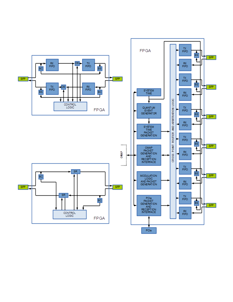
Usually at the heart of all modern day power electronics designs specifically those dealing with the control of power flow using switching devices, one find in use an FPGA (Field Programmable Gate Array) as the interface between the processor (typically a DSP) and the switch mode power converter.
In the case of the M2LC, the power converter consists of potentially a large number of stacked switching elements that must operate together in a precise manor governed by a central control unit. Being that the number of elements to be stacked can create a design capable of sustaining a DC bus of many thousands of volts, signal isolation between each of the switching elements is required.
Also, the voltage contribution of each element is typically in excess of 1000 VDC which prohibits the use of a simple opto-isolators.
It turns out that modern FPGA’s such as the Xilinx® Series 7™ and Altera® Cyclone™ family contain integrated SERDES interfaces that are capable of operating at a minimum of 1 GHz. This coupled with Glass Fiber Optic transceivers and cables such as SFP+ allow for a very robust (high noise immunity), high throughput form of communications between each of the switch elements and the central controller.
More information on this can be found here.
