A new strategy for a faster time-to-market
We have heard of the term Rapid Prototyping. This phrase has been around since the 80s. When applied to electronic design, more times then not the end result is a abstract representation of the envisioned product. This is usually because the development approach used is top-down in nature.
Nevertheless some degree of top down organization is necessary so as to convey the validity of the design as well as maintain a design schedule.
What is needed is an approach that combines a bottom-up physical design that best represents the final product with one having a top-down organization.
 This idea can best be described using the M2LC hardware design proposal provided in the paper High Performance M2LC System. A simple diagram of the circuit is shown at the right.
We need to create the closest possible representation of the final system using components that are readily available. This satisfies our bottom-up requirement.
At the same time, we need to provide a capability of allowing for the research and testing of different control algorithms required to satisfy a top-down design methodology.
We do this by substituting the abstract blocks labeled M2LC cell and CTRL module with components that can best represent the final design.
The most complicated block such as the CTRL module must possess one or more processors, a programmable gate array (FPGA) and a fiber-optic interface.
Equally important is the blocks labeled M2LC cell which infer the need for the use of a gate array as well as a fiber optic interface that connects to the CTRL cell.
To complete the system we need components that represent the IGBT half-bridges that are contained in each of the blocks labeled M2LC cell. The components used here have a less stringent requirement for qualification because they need only represent that which would be used in the final design. In fact, for safety reasons, the ratings of these component would be greatly reduced being that an actual M2LC system is typically required to operate an many thousands of volts and hundreds of amps.
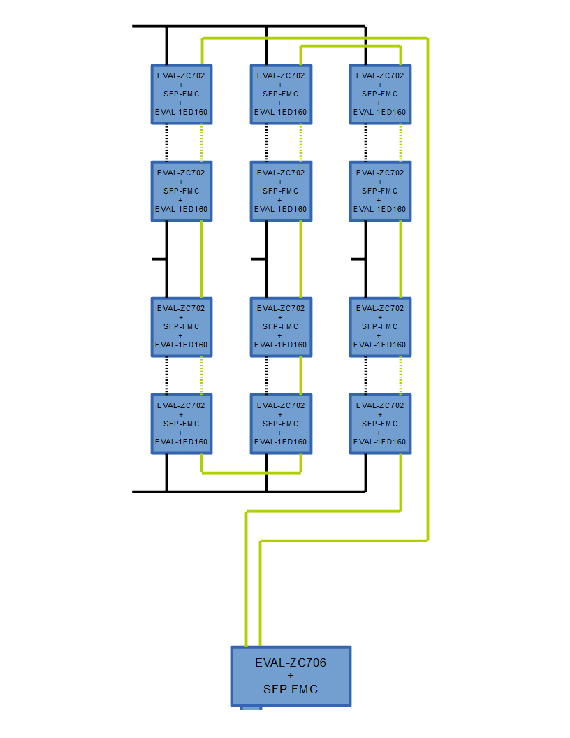
With this in place, we define a development system that can best represent the M2LC as a basis for a final design. A diagram of this system is shown on the right.
The system contains the following components.
For the CTRL module, a Xilinx™ ZC706 Zynq® evaluation board and a plug-on dual SFP fiber FMC interface board. The Zynq contains a dual ARM processor and integrated FPGA. Combined with FMC interface board the implementation for our representative CTRL module is complete. This evaluation board can also be plugged into a PCIe slot on a PC, the use of this will be explained below.
For each of the M2LC cell control circuits, a logical selection would be the Xilinx™ AC701 Artix-7® evaluation board, a plug-on dual SFP fiber FMC interface board and a plug-on analog/digital FMC interface board.
For the representative implement of the M2LC cell power circuits, an Infineon™ EVAL-1EDI60I12AF half bridge converter and two power film capacitors would be used.
To complete the development system, we need to add a transformer and rectifier to generate the DC bus voltage.
Glass Fiber optical cable operating at 1 GHz would connect the each of the M2LC cells and CTRL modules.
For safety reasons during the development stage, each M2LC cell is designed to work at a greatly reduced bus voltage. For the most part, this operating constraint would not effect the development of control algorithms.
The PCIe connection on the CTRL module (represented by the Zynq board) would allow connection on a PC that would be setup to run real time development OS’s such as LabVIEW® Real-Time™ or Simulink® Desktop Real-Time™. This is the top-down development interface for evaluating any of the proposed control algorithms used to control the M2LC.
The JTAG interface on the CTRL module would provide direction connection to the Xilinx® Zynq development software. This provides our bottom-up development interface for the writing of the code that implements the selected control algorithm.
If the real time development OS is designed to run on a separate processor core along side Windows™, one PC can be used for both the JTAG and PCIe development interfaces.
The development of the control logic running on the Artix boards used to implement each of the M2LC cells would require the use of a PC based Xilinx JTAG interface and FPGA development software together with a hardware description language simulator such as Mentor Graphics® ModelSim™. The firmware designed here is used to support both the PCIe based and JTAG based development of the CTRL module described above.
If all goes well, we end up with a system for which the power circuits needs only to be upsized for the actual implementation. As for the control components, we need only refer to the Xilinx Zynq and Artix evaluation board schematics and select the components on these boards that are required to fulfill the design in question.
